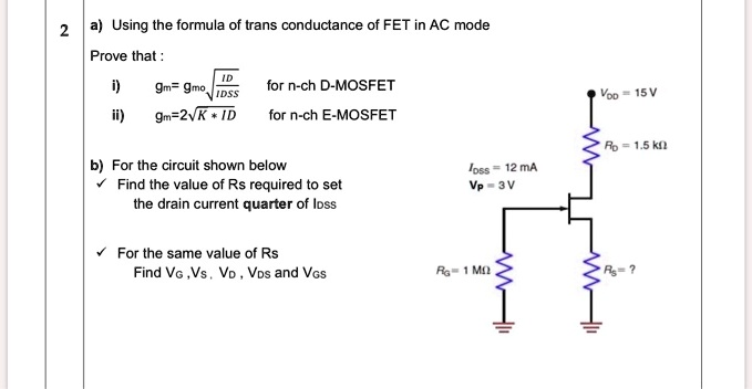
a) Using the formula of transconductance of FET in AC mode, prove that: i) for n-channel D-MOSFET, gm = 2√(KID) ii) for n-channel E-MOSFET, Rp = 1.5k b) For the circuit shown below, find the value of Rs required to set the drain current at a quarter of loss. Loss = 12mA, Vp = 3V For the same value of Rs, find VGVs, VoVos, and VGs. R = 1MO
The Correct Answer and Explanation is:
Correct Answer
Part a) Proofs:
The proofs for the transconductance formulas are detailed in the explanation below by differentiating the standard current equations for D-MOSFETs and E-MOSFETs.
Part b) Circuit Analysis:
- The required value of the source resistor is Rs = 500 Ω.
- The DC voltage values are:
- VGS = -1.5 V
- VG = 0 V
- VS = 1.5 V
- VD = 10.5 V
- VDS = 9.0 V
Detailed Explanation
This problem involves two parts: first, deriving the AC transconductance (g_m) formulas for different types of MOSFETs, and second, performing a DC analysis of a JFET/D-MOSFET self-bias circuit.
Part a) Transconductance Proofs
i) For n-channel D-MOSFET:
The transconductance, g_m, is defined as the change in drain current (I_D) with respect to the change in gate-to-source voltage (V_GS), which is mathematically expressed as the partial derivative g_m = ∂I_D / ∂V_GS.
The drain current for a D-MOSFET (or JFET) in the saturation region is given by the Shockley equation:
I_D = I_DSS * (1 – V_GS / V_p)²
Differentiating I_D with respect to V_GS using the chain rule yields:
g_m = I_DSS * 2 * (1 – V_GS / V_p) * (-1 / V_p)
g_m = (-2 * I_DSS / V_p) * (1 – V_GS / V_p)
The maximum transconductance, g_mo, occurs at V_GS = 0. Substituting V_GS = 0 into the equation gives:
g_mo = -2 * I_DSS / V_p
By substituting g_mo back into the general g_m equation, we get:
g_m = g_mo * (1 – V_GS / V_p)
From the original Shockley equation, we can also express (1 – V_GS / V_p) as √(I_D / I_DSS). Substituting this relationship into the equation for g_m proves the required formula:
g_m = g_mo * √(I_D / I_DSS)
ii) For n-channel E-MOSFET:
The drain current for an E-MOSFET in saturation is given by:
I_D = K * (V_GS – V_th)², where K is a device constant and V_th is the threshold voltage.
Differentiating I_D with respect to V_GS:
g_m = ∂I_D / ∂V_GS = K * 2 * (V_GS – V_th)
From the E-MOSFET current equation, we can write (V_GS – V_th) = √(I_D / K). Substituting this into the g_m equation:
g_m = 2 * K * √(I_D / K)
g_m = 2 * √(K² * I_D / K)
g_m = 2 * √(K * I_D)
Part b) Circuit DC Analysis
The circuit shown is a self-bias configuration for an n-channel JFET/D-MOSFET. The provided parameters are I_DSS = 12 mA, V_p = -3 V (for an n-channel device), and R_D = 1.5 kΩ.
1. Find the value of Rs:
The problem requires setting the drain current I_D to a quarter of I_DSS.
I_D = I_DSS / 4 = 12 mA / 4 = 3 mA
To find the V_GS required for this I_D, we use the Shockley equation:
I_D = I_DSS * (1 – V_GS / V_p)²
3 mA = 12 mA * (1 – V_GS / (-3 V))²
1/4 = (1 + V_GS / 3)²
Taking the square root of both sides: ±1/2 = 1 + V_GS / 3. For operation, V_GS must be between V_p (-3V) and 0. This condition is met for the negative root.
1/2 = 1 + V_GS / 3 => V_GS / 3 = -1/2 => V_GS = -1.5 V
In a self-bias circuit, the gate current I_G is approximately zero. Therefore, there is no voltage drop across R_G, and the gate voltage V_G is 0 V. The source voltage is V_S = I_D * R_s.
The gate-to-source voltage is V_GS = V_G – V_S = 0 – I_D * R_s = -I_D * R_s.
We can now solve for R_s:
-1.5 V = -(3 mA) * R_s
R_s = 1.5 V / 3 mA = 0.5 kΩ or 500 Ω.
2. Find VG, VS, VD, VDS, and VGS:
Using the calculated value of R_s = 500 Ω and the operating point I_D = 3 mA:
- VGS: Already calculated to establish the operating point. VGS = -1.5 V.
- VG: As established, with no gate current, VG = 0 V.
- VS: V_S = I_D * R_s = 3 mA * 500 Ω = 1.5 V. (Check: V_GS = V_G – V_S = 0 V – 1.5 V = -1.5 V. Correct.)
- VD: The drain voltage is calculated from the supply voltage and the drop across R_D.
V_D = V_DD – I_D * R_D = 15 V – (3 mA * 1.5 kΩ) = 15 V – 4.5 V = 10.5 V. - VDS: The drain-to-source voltage is the difference between the drain and source voltages.
V_DS = V_D – V_S = 10.5 V – 1.5 V = 9.0 V.
