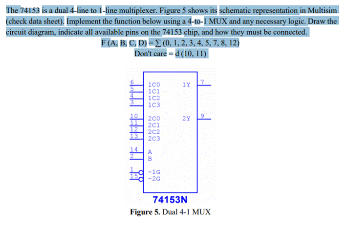
The 74153 Is A Dual 4-Line To 1-Line Multiplexer. Figure 5 Shows Its Schematic Representation In Multisim (Check Data Sheet). Implement The Function Below Using A 4-To-1 MUX And Any Necessary Logic. Draw The Circuit Diagram, Indicate All Available Pins On The 74153 Chip, And How They Must Be Connected. F (A, B, C, D) = (0, 1, 2, 3, 4, 5, 7, 8, 12) Don’t Care
The Correct Answer and Explanation is:
✅ Correct Implementation using 74153 MUX
The 74153 is a dual 4-to-1 multiplexer, meaning it contains two independent 4-input multiplexers, each with two select lines (A and B) and independent enable lines (~1G and ~2G).
🎯 Objective
You are asked to implement the Boolean function:
F(A, B, C, D) = Σ(0, 1, 2, 3, 4, 5, 7, 8, 12), with Don’t Cares = d(10, 11)
using a 4-to-1 multiplexer (74153) and necessary logic.
🔧 Strategy to Use 4-to-1 MUX
A 4-to-1 MUX selects one of four inputs (I0–I3) based on 2 select lines (say A and B).
You must map a 4-variable function (A, B, C, D) into a 4-to-1 MUX. To do this:
- Use C and D as select lines (2 bits → 4 options)
- Use A and B to build the 4 data inputs (I0–I3)
- For the 74153, we’ll use 1Y output from the upper MUX (1C0–1C3, ~1G)
✅ Implementation Steps
- Assign Select Inputs:
- Connect C to pin 2 (Select A)
- Connect D to pin 14 (Select B)
- Enable the MUX:
- Connect ~1G (pin 1) to GND (active LOW enable)
- Connect ~2G (pin 15) to VCC (disable lower MUX)
- Implement the logic for inputs I0–I3 (1C0 to 1C3):
- Create 4-variable Karnaugh map of F(A, B, C, D)
- For each combination of CD = 00, 01, 10, 11, determine 1C0–1C3 as functions of A and B
| C | D | I | Minterms for CD | Required function (AB domain) |
|---|---|---|---|---|
| 0 | 0 | 1C0 | 0,1,4,5 | F = A’B’ + A’B + AB’ + AB = 1 |
| 0 | 1 | 1C1 | 2,3 | F = A’B’ + A’B = A’ |
| 1 | 0 | 1C2 | 8,12 | F = A’B’ + AB’ = B’ |
| 1 | 1 | 1C3 | 7 | F = A B |
- Implement logic for I0 to I3:
- 1C0 = 1 → Connect to VCC
- 1C1 = A’ → Invert A
- 1C2 = B’ → Invert B
- 1C3 = A·B → Use AND gate with A and B
- Connect Outputs:
- Use pin 7 (1Y) as the output F(A,B,C,D)
🔌 Pin Connections (Summary):
| Pin | Connection |
|---|---|
| 1 (~1G) | GND |
| 2 (A) | C |
| 14 (B) | D |
| 3 (1C0) | VCC |
| 4 (1C1) | A’ (use NOT gate) |
| 5 (1C2) | B’ (use NOT gate) |
| 6 (1C3) | A·B (use AND gate) |
| 7 (1Y) | Output F |
| 15 (~2G) | VCC |
| Other 2Cx inputs | Unused (tie to GND or VCC safely) |
| VCC, GND | Standard power |
🧠 Summary Explanation
To implement a 4-variable Boolean function using a 4-to-1 multiplexer like the 74153, we strategically assign two of the variables to serve as select inputs, while the remaining variables define the logic for the multiplexer’s data inputs. The function provided, F(A, B, C, D) = Σ(0, 1, 2, 3, 4, 5, 7, 8, 12), can be expressed using a Karnaugh Map, which shows how output F varies with different combinations of inputs.
By assigning C and D to the MUX’s select lines, we fix them to select one of four data lines (I0 through I3). Then, using the truth table and minterms, we determine the logic each data input must represent in terms of A and B. For example, for select input CD = 00 (I0), F is true regardless of A and B, so I0 is tied to logic HIGH (1). Similarly, I1 = A’, I2 = B’, and I3 = A·B. These logic expressions are built using basic gates (NOT, AND) and connected to the appropriate MUX inputs.
We enable only the first MUX (by grounding ~1G), and disable the second MUX by tying ~2G to VCC. The final output F is taken from pin 7 (1Y) of the MUX. This design uses minimal hardware and demonstrates efficient implementation of a complex function using a multiplexer.